- 您现在的位置:买卖IC网 > Sheet目录3822 > PIC18F4525-I/ML (Microchip Technology)IC MCU FLASH 24KX16 44QFN
PIC18F2525/2620/4525/4620
DS39626E-page 16
2008 Microchip Technology Inc.
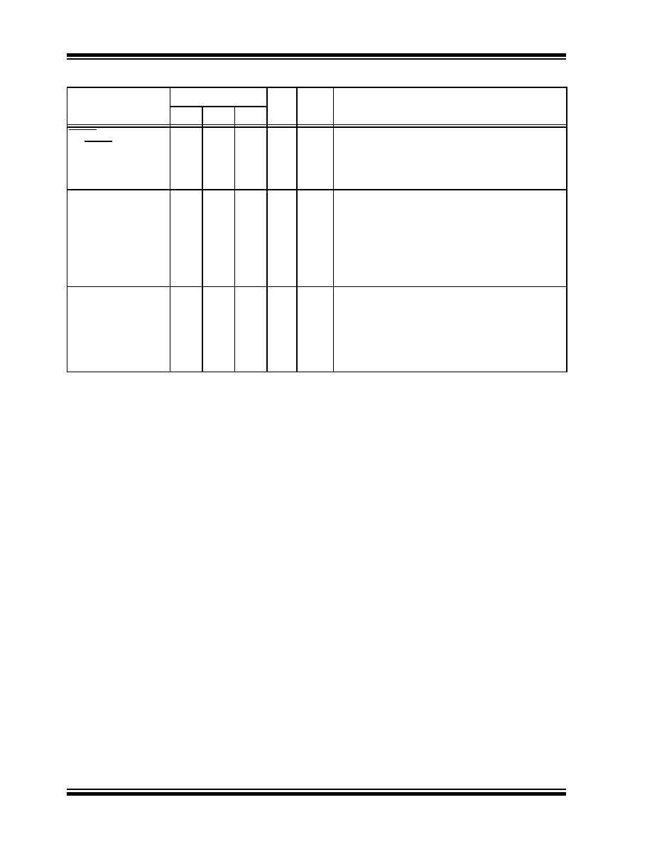
TABLE 1-3:
PIC18F4525/4620 PINOUT I/O DESCRIPTIONS
Pin Name
Pin Number
Pin
Type
Buffer
Type
Description
PDIP
QFN
TQFP
MCLR/VPP/RE3
MCLR
VPP
RE3
118
18
I
P
I
ST
Master Clear (input) or programming voltage (input).
Master Clear (Reset) input. This pin is an active-low
Reset to the device.
Programming voltage input.
Digital input.
OSC1/CLKI/RA7
OSC1
CLKI
RA7
13
32
30
I
I/O
ST
CMOS
TTL
Oscillator crystal or external clock input.
Oscillator crystal input or external clock source input.
ST buffer when configured in RC mode;
analog otherwise.
External clock source input. Always associated with
pin function OSC1. (See related OSC1/CLKI,
OSC2/CLKO pins.)
General purpose I/O pin.
OSC2/CLKO/RA6
OSC2
CLKO
RA6
14
33
31
O
I/O
—
TTL
Oscillator crystal or clock output.
Oscillator crystal output. Connects to crystal
or resonator in Crystal Oscillator mode.
In RC mode, OSC2 pin outputs CLKO which
has 1/4 the frequency of OSC1 and denotes
the instruction cycle rate.
General purpose I/O pin.
Legend: TTL = TTL compatible input
CMOS = CMOS compatible input or output
ST = Schmitt Trigger input with CMOS levels
I
= Input
O
= Output
P
= Power
Note 1:
Default assignment for CCP2 when the CCP2MX Configuration bit is set.
2:
Alternate assignment for CCP2 when the CCP2MX Configuration bit is cleared.
3:
For the QFN package, it is recommended that the bottom pad be connected to VSS.
发布紧急采购,3分钟左右您将得到回复。
相关PDF资料
DSPIC30F2023-30I/ML
IC DSPIC MCU/DSP 12K 44QFN
PIC16LF767-I/ML
IC PIC MCU FLASH 8KX14 28QFN
PIC18LF2320-I/SO
IC MCU FLASH 4KX16 EEPROM 28SOIC
PIC18F4458-I/ML
IC PIC MCU FLASH 12KX16 44QFN
DSPIC33FJ64GP706A-I/PT
IC DSPIC MCU/DSP 64K 64-TQFP
PIC16F874-20/P
IC MCU FLASH 4KX14 EE 40DIP
DSPIC33FJ64GP706-I/PT
IC DSPIC MCU/DSP 64K 64TQFP
PIC24HJ128GP210-I/PT
IC PIC MCU FLASH 128KB 100TQFP
相关代理商/技术参数
PIC18F4525-I/P
功能描述:8位微控制器 -MCU 48KB 3968 RAM 36I/O RoHS:否 制造商:Silicon Labs 核心:8051 处理器系列:C8051F39x 数据总线宽度:8 bit 最大时钟频率:50 MHz 程序存储器大小:16 KB 数据 RAM 大小:1 KB 片上 ADC:Yes 工作电源电压:1.8 V to 3.6 V 工作温度范围:- 40 C to + 105 C 封装 / 箱体:QFN-20 安装风格:SMD/SMT
PIC18F4525-I/P
制造商:Microchip Technology Inc 功能描述:IC 8BIT FLASH MCU 18F4525 DIP40
PIC18F4525-I/PT
功能描述:8位微控制器 -MCU 48KB 3968 RAM 36I/O RoHS:否 制造商:Silicon Labs 核心:8051 处理器系列:C8051F39x 数据总线宽度:8 bit 最大时钟频率:50 MHz 程序存储器大小:16 KB 数据 RAM 大小:1 KB 片上 ADC:Yes 工作电源电压:1.8 V to 3.6 V 工作温度范围:- 40 C to + 105 C 封装 / 箱体:QFN-20 安装风格:SMD/SMT
PIC18F4525-I/PT
制造商:Microchip Technology Inc 功能描述:IC 8BIT FLASH MCU 18F4525 TQFP44
PIC18F4525T-I/ML
功能描述:8位微控制器 -MCU 48KB 3968 RAM 36I/O RoHS:否 制造商:Silicon Labs 核心:8051 处理器系列:C8051F39x 数据总线宽度:8 bit 最大时钟频率:50 MHz 程序存储器大小:16 KB 数据 RAM 大小:1 KB 片上 ADC:Yes 工作电源电压:1.8 V to 3.6 V 工作温度范围:- 40 C to + 105 C 封装 / 箱体:QFN-20 安装风格:SMD/SMT
PIC18F4525T-I/PT
功能描述:8位微控制器 -MCU 48KB 3968 RAM 36I/O RoHS:否 制造商:Silicon Labs 核心:8051 处理器系列:C8051F39x 数据总线宽度:8 bit 最大时钟频率:50 MHz 程序存储器大小:16 KB 数据 RAM 大小:1 KB 片上 ADC:Yes 工作电源电压:1.8 V to 3.6 V 工作温度范围:- 40 C to + 105 C 封装 / 箱体:QFN-20 安装风格:SMD/SMT
PIC18F452-BL
制造商:POWERLITE SYSTEMS 功能描述:BOOTLOADER PIC18F452 FOR FLASHLAB 制造商:POWERLITE SYSTEMS 功能描述:BOOTLOADER, PIC18F452, FOR FLASHLAB 制造商:POWERLITE SYSTEMS 功能描述:BOOTLOADER, PIC18F452, FOR FLASHLAB, Silicon Manufacturer:Powerlite Systems, Cor 制造商:POWERLITE SYSTEMS 功能描述:PIC18F452 W/ BOOTLOADER, FOR FLASHLAB, Silicon Manufacturer:Powerlite Systems, Core Architecture:PIC, Core Sub-Architecture:PIC18F, Kit Contents:Board , RoHS Compliant: Yes
PIC18F452-E/L
功能描述:8位微控制器 -MCU 32KB 1536 RAM 34I/O RoHS:否 制造商:Silicon Labs 核心:8051 处理器系列:C8051F39x 数据总线宽度:8 bit 最大时钟频率:50 MHz 程序存储器大小:16 KB 数据 RAM 大小:1 KB 片上 ADC:Yes 工作电源电压:1.8 V to 3.6 V 工作温度范围:- 40 C to + 105 C 封装 / 箱体:QFN-20 安装风格:SMD/SMT